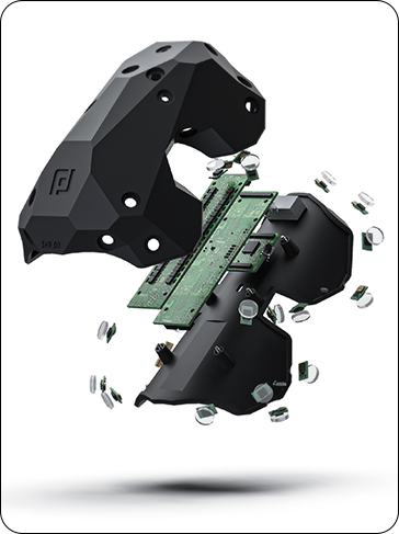


What we package
- Board outlines, stacking, and mounting
- Connectors, cable routing, and strain relief
- Batteries, displays, and user inputs
- Antennas and RF keep-out zones
- Heat paths from components to the enclosure
Designed with the board, not around it
We develop packaging alongside PCB design and layout, so board outlines, tall components, and connectors fit the enclosure from the first prototype. Heat is planned with thermal management, and wireless products get the same attention through antenna integration.
Protected for the real world
For products that face shock, vibration, and weather, packaging works together with rugged enclosure design and sealing. Electronics packaging is part of our mechanical engineering services.
Frequently asked questions
Can you package electronics designed by another team?
Yes. We can design the enclosure and internal packaging around your boards, or work with your electrical team to adjust outlines and connectors.
How do you avoid conflicts between boards and housings?
We share 3D models between electrical and mechanical design as the layout evolves and review fit before prototypes are built.
Do you design cable routing?
Yes. We define cable routing, lengths, connectors, and strain relief as part of the packaging design.
Can you make an existing product smaller?
Often. Board stacking, connector choices, and component placement can significantly reduce size. We can review your current design and recommend options.



Related capabilities
Meet with us
Discuss your current development projects, approach, team, and goals

We'll propose the initial step
Our team defines the first body of work based on your business realities
See results
Realize the benefits of an award winning team focused on your project


